Molecular Electronics
2019 Publications
Wang, Z.; Zhuang, X.; Chen, Y.; Wang, B.; Huang, W.; Marks, T.J.; Facchetti, A. Cinnamate-Functionalized Natural Carbohydrates as Photopatternable Gate Dielectrics for Organic Transistors, Chem. Mater., 2019, 31, 7608-7617. DOI: 10.1021/acs.chemmater.9b02413
Zheng, D.; Peng, R.; Wang, G.; Logsdon, J.L.; Wang, B.; Hu, X.; Chen, Y.; Dravid, V.P.; Wasielewski, M.R.; Yu, J.; Huang, W.; Ge, Z.; Marks, T.J.; Facchetti, A.; Simultaneous Bottom-up Interfacial and Bulk Defect Passivation in Highly Efficient Planar Perovskite Solar Cells using Non-Conjugated Small-Molecule Electrolytes, Adv. Mater. 2019, in press. DOI:10.1002/adma.201903239
Zhang, X.; Wang, B.; Huang, W.; Wang, G.; Zhu, W.; Wang, Z.; Zhang, W.; Facchetti, A.; Marks, T.J.; Oxide-Polymer Heterojunction Diodes with a Nanoscopic Phase Separated Insulating Layer, Nano Lett., 2019, 19, 471–476. DOI: 10.1021/acs.nanolett.8b04284.
Selected Previous Publications
Zeng, L.; Turrisi, R.; Fu, B.; Emery, J.D.; Walker, A.R.; Ratner, M.A.; Hersam, M.C.; Facchetti, A.F.; Marks, T.J.; Bedzyk, M.J.; Measuring Dipole Inversion in Self-Assembled Nano-Dielectric Molecular Layers, ACS Appl. Mater. Inter., 2018, 10, 6484–6490. DOI: 10.1021/acsami.7b16160.
Eckstein, B.J.; Melkonyan, F.S.; Manley, E.F.; Fabiano, S.; Mouat, A.R.; Chen, L.X.; Facchetti, A.; Marks, T.J.; Naphthalene Bis(4,8-diamino-1,5-dicarboxyl)amide Building Block for Semiconducting Polymers, J. Am. Chem. Soc. 2017, 139, 14356–14359. DOI: 10.1021/jacs.7b07750
Eckstein, B. J.; Melkonyan, F. S.; Zhou, N.; Manley, E. F.; Smith, J.; Timalsina, A.; Chang, R. P. H.; Chen, L. X.; Facchetti, A.; Marks, T. J., Buta-1,3-diyne-Based π-Conjugated Polymers for Organic Transistors and Solar Cells. Macromolecules 2017, 50 (4), 1430-1441.
Wang, G.; Huang, W.; Eastham, N.D.; Manley, E.F.; Zeng, L.; Wang, B.; Zhang, X.; Chen, Z.; Li, R.; Melkonyan, F.; Chen, L.X.; Bedzyk, M.J.; Facchetti, A.; Marks, T.J.; Aggregation Control in Brush-Printed Conjugated Polymer Films and Implications for Efficient Charge Transport, Proc. Nat. Acad. Sci. USA, 2017, 114, E10066-E10073. DOI: 10.1073/pnas.1713634114.
Wang, B.; Di Carlo, G.; Turrisi, R.; Zeng, L.; Stallings, K.; Bedzyk, M.J.; Beverina, L.; Marks, T.J.; Facchetti, A.; Dipole Moment Inversion Effects in Self-Assembled Nanodielectrics for Thin Film Transistors, Chem. Mater. 2017, 29, 9974–9980. DOI: 10.1021/acs.chemmater.7b03397.
Huang, W.; Zhuang, X.; Melkonyan, F.S.; Wang, B.; Zeng, L.; Wang, G.; Han, S.; Bedzyk, M.; Yu, J.; Marks, T.J.; Facchetti, A.; UV/Ozone Induced Interfacial Trap Effects in Organic Transistors for High-Sensitivity NO2 Detection, Adv. Mater. 2017, 29, 1701706. DOI: 10.1002/adma.201701706.
Eckstein, B.J.; Melkonyan, F.S.; Zhou, N.; Manley, E.F.; Smith, J.; Timalsina, A.; Chang, R.P.H.; Chen, L.X.; Facchetti, A.; Marks, T.J. Buta-1,3-diyne Based π-Conjugated Polymers for Organic Transistors and Solar Cells, Macromolecules, 2017, 50,1430–1441. DOI: 10.1021/acs.macromol.6b02702.
Heitzer, H. M.; Marks, T. J.; Ratner, M. A., Computation of Dielectric Response in Molecular Solids for High Capacitance Organic Dielectrics. Acc. Chem. Res. 2016, 49 (9), 1614-1623.
Heitzer, H. M.; Marks, T. J.; Ratner, M. A., Molecular-Donor-Bridge-Acceptor Strategies for High-Capacitance Organic Dielectric Materials. J. Am. Chem. Soc. 2015, 137 (22), 7189-7196.
Usta, H.; Facchetti, A.; Marks, T. J., n-Channel Semiconductor Materials Design for Organic Complementary Circuits. Acc. Chem. Res. 2011, 44 (7), 501-510.
DiBenedetto, S. A.; Facchetti, A.; Ratner, M. A.; Marks, T. J., Molecular Self-Assembled Monolayers and Multilayers for Organic and Unconventional Inorganic Thin-Film Transistor Applications. Adv. Mater. 2009, 21 (14-15), 1407-1433.
Wang, L.; Yoon, M.-H.; Lu, G.; Yang, Y.; Facchetti, A.; Marks, T. J., High-performance transparent inorganic-organic hybrid thin-film n-type transistors. Nat. Mater. 2006, 5 (11), 893-900.
Organic/Inorganic Hybrid Materials for Modern Electronics
The D-Team is focused on the search of new organic/inorganic functional materials for modern electronics applications. One of the main goals of our group is the fabrication of flexible/stretchable electronic devices using inexpensive, high-throughput, and scalable processing technologies for circuit fabrication. Applications for these materials could include printed circuits, rollable newspapers, head-up displays, real-time wearable displays, spatial light modulators…
Organic Semiconducting Materials
In the organic electronic field, our group has pioneered the development of n-type (electron transport) oligothiophene semiconductors, and has presented one of the highest mobilities reported to date for air-stable arylene-based semiconductors. Furthermore, a great number of oligomer and polymer materials have been and are being synthesized in our group, which are both air stable and solution processed. We continue to look for new semiconductors and small molecules for transistor applications.
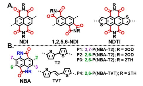
Figure 1. (A) Naphthalene diimido-based building blocks. (B) NBA core and polymer structures.
Self-Assembled NanoDielectrics (SANDs)
Our group is trying to develop new dielectrics for low operating voltage of TFTs (Thin-Film Transistors). Self-assembled nanodielectrics (SANDs) are representative examples. These dielectrics are compatible with organic semiconductors, single-walled carbon nanotubes (SWCNT), Single crystal Si nanoribbons, and inorganic semiconductors such as metal oxide nanowires, as well as thin films. Furthermore, the resulting SAND-based TFTs operate at extremely low voltages and exhibit greater mobility of FETs than analogous TFTs fabricated with conventional SiO2 gate dielectrics owing to the unique SAND combination of high dielectric constant, nanometer thickness, low gate leakage current, and low interface trap state densities.
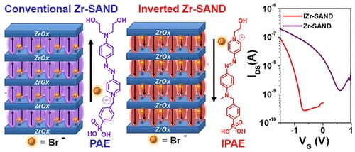
Figure. Dielectric stacks comprising four-chromophore/ZrOx layers on top of the ZrOx (p-ZrOx) primer film, and transfer plots of pentacene OTFTs on cZr-SAND and cIZr-SAND.
Advanced Printing process
Shear-printing of electroactive polymers using natural brushes is a promising film deposition technique for printed electronics capable of microstructure control and electrical properties enhancement over large areas. Nevertheless, the interplay between film printing parameters, microstructure development, and charge transport is not well-understood. We report that natural brush-printing greatly enhances charge transport by as much as 5.7× through control of polymer nanofibril aggregate growth and backbone alignment, attributable to the oriented squamae of the natural hair. However, while brush shear-induced aggregation enhances charge transport, we show that backbone alignment alone does not guarantee charge transport anisotropy. These results provide additional understanding of shear-induced enhanced charge transport and set processing guidelines for high-performance printed organic circuitry.
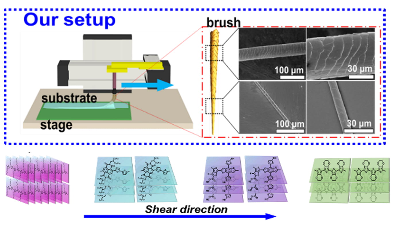
Figure. Schematic of brush-printing setup including SEM images of the brush natural hair with squamae structures, and the molecular chain stacking of the brush-printed films, with the arrow indicating the brush-printing direction.
Featured Covers