Transparent Oxides
2019 Publications
Wang, B.; Guo, P.; Zeng, L.; Sil, A.; Huang, W.; Leonardi, M.J.; Zhang, X.; Wang, G.; Yu, X.; Bedzyk, M.J.; Schaller, R.D.; Marks, T.J.; Facchetti, A.; Ultrafast, scalable fabrication of solution-processed metal oxides for thin-film electronics, Proc. Natl. Acad. Sci. USA, 2019, 116, 9230-9238. DOI: 10.1073/pnas.1901492116.
Moffitt, S.L.; Stallings, K.L.; Falduto, A.F.; Lee, W.; Buchholz, D.B.; Wang, B.; Ma, Q.; Chang, R.P.H.; Marks, T.J.; Bedzyk, M.J.; Processing, structure, and Transistor Performance:Combustion Synthesis verus Pulsed Laser Growth of Amorphous Oxides, ACS Appl. Electron. Mater. 2019, 1, 4, 548–557. DOI: 10.1021/acsaelm.9b00012.
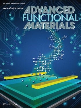
Zheng, D.; Wang, G.; Huang, W.; Wang, B.; Ke, W.; Logsdon, J.L.; Wang, H.; Wang, Z.; Zhu, W.; Wasielewski, M.R.; Kanatzidis, M.G.; Yu, J.; Marks, T.J.; Facchetti, A.; Combustion synthesized zinc oxide electron-transporting layer for efficient and stable perovskite solar cells, Adv. Funct. Mater. 2019, 29, 1900265.
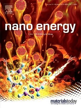
Huang, W.; Wang, G.; Luo, C.; Xu, Y.; Xu, Y.; Eckstein, B.J.; Chen, Y.; Wang, B.; Huang, J.; Kang, Y.; Wu, J.; Dravid, V.P.; Facchetti, A.; Marks, T.J.; Controllable Growth of LiMn2O4 by Combustion Synthesis for High Performance Li-ion Batteries, Nano Energy, 2019, 64, 103936. DOI: doi.org/10.1016/j.nanoen.2019.103936
Chen, Y.; Huang, W.; Sangwan, V.K.; Wang, B.; Zeng, L.; Wang, G.; Huang, Y.; Lu, Z.; Bedzyk, M.J.; Hersam, M.C.; Marks, T.J.; Facchetti, A.; Polymer Doping Enables Two-Dimensional Electron Gas for High-Performance Homojunction Oxide Thin-Film Transistors, Adv. Mater. 2019, 31,1805082. DOI:10.1002/adma.201805082.
Selected Previous Publications
Zeng, L.; Moghadam, M.M; Buchholz, D.B.; Li, R.; Keane, D.T.; Dravid, V.P.; Chang, R.P.H.; Voorhees, P.W.; Marks, T.J.; Bedzyk, M.J.; Processing-Dependent Thermal Stability of a Prototypical Amorphous Metal Oxide, Phys. Rev. Mater. 2018, 2, 053401-053410. DOI: 10.1103/PhysRevMaterials.2.053401
Chen, Y.; Wang, B.; Huang, W.; Zhang, X.; Wang, G.; Leonardi, M.; Huang, Y.; Lu, Z.; Marks, T.J.; Facchetti, A.; Nitroacetylactone as a (co)Fuel for the Combustion Synthesis of High-Performance Indium-Gallium-Zinc Oxide Transistors, Chem. Mater. 2018, 30103323-3329. DOI: 10.1021/acs.chemmater.8b00663.
Zhang, X.; Wang, B.; Huang, W.; Zeng, L.; Wang, G.; Zhu W.; Chen, Y.; Bedzyk, M.J.; Zhang, W.; Medvedeva, J.E.; Facchetti, A.; Marks, T.J.; Boron Doping in Solution-Processed Metal Oxide Films for High-Performance Thin-Film Transistors–Theory and Experiment, J. Am. Chem. Soc. 2018, 140, 12501–12510. DOI: 10.1021/jacs.8b06395.
Huang, W.; Guo, P.; Zeng, L.; Li, R.; Wang, B.; Wang, G.; Zhang, X.; Chang, R.P.H.; Yu, J.; Bedzyk, M.J.; Marks, T.J.; Facchetti, A.; Metal Composition and Polyethylenimine Doping Capacity Effects on Semiconducting Metal Oxide-Polymer Blend Charge Transport, J. Am. Chem. Soc., 2018, 140, 5457–5473. DOI: 10.1021/jacs.8b01252.
Wang, B.; Huang, W.; Chi, L.; Al-Hashimi, M.; Marks, T.J.; Facchetti, A.; High-k Gate Dielectrics for Emerging Flexible and Stretchable Electronics, Chem. Rev. 2018, 118, 5690-5754. DOI: 10.1021/acs.chemrev.8b00045.
Yu, X. G.; Marks, T. J.; Facchetti, A., Metal oxides for optoelectronic applications. Nat. Mater. 2016, 15 (4), 383-396.
Wang, B.; Zeng, L.; Huang, W.; Melkonyan, F.; Sheets, W.C.; Chi, L.; Bedzyk, M.J.; Marks, T.J.; Facchetti, A.; Carbohydrate-Assisted Combustion Synthesis to Realize High-Performance Oxide Transistors, J. Am. Chem. Soc., 2016, 138, 7067–7074. DOI: 10.1021/jacs.6b02309
Huang, W.; Zeng, L.; Yu, X.; Guo, P.; Wange, B.; Ma, Q.; Chang, R.P.H.; Yu, J.; Bedzyk, M.; Marks, T.J.; Facchetti, A.; High-performance metal oxide transistors via polyethyleneimine doping of the channel layer, Adv. Funct. Mater. 2016, 26,6179-6187. DOI: 10.1002/adfm.201602069.
Yu, X.; Zeng, L.; Zhou, N.; Guo, P.; Shi, F.; Buchholz, D.B.; Yu, J.; Dravid, V.P.; Chang, R.P.H; Bedzyk, M.; Marks, T.J.; Facchetti, A.; Ultra-Flexible, “Invisible” Thin Film Transistors Enabled by Amorphous Metal Oxide/Polymer Channel Layer Blends, Adv. Mater. 2015, 27, 2390–2399. DOI: 10.1002/adma.201405400.
Yu, X.; Smith, J.; Zhou, N. J.; Zeng, L.; Guo, P. J.; Xia, Y.; Alvarez, A.; Aghion, S.; Lin, H.; Yu, J. S.; Chang, R. P. H.; Bedzyk, M. J.; Ferragut, R.; Marks, T. J.; Facchetti, A., Spray-combustion synthesis: Efficient solution route to high-performance oxide transistors. Proc. Natl. Acad. Sci. USA, 2015, 112 (11), 3217-3222.
Kim, M.-G.; Kanatzidis, M. G.; Facchetti, A.; Marks, T. J., Low-temperature fabrication of high-performance metal oxide thin-film electronics via combustion processing. Nat. Mater. 2011, 10 (5), 382-388.
Solution Processed Transparent Oxide Thin Films
Metal oxide (MO) (semi)conductors have attracted great attention for next-generation electronics because of their high carrier mobilities, optical transparency, and air stability. Nowadays, commercialized metal oxide (semi)conductors are fabricated by physical vapor deposition techniques, which are expensive and require photolithographic patterning, thus limiting roll-to-roll fabrication. In recent years, solution processing has emerged as an alternative way to deposit/pattern metal oxide (semi)conductors, but transistor performance is below that of physical deposited MOs. Solution-processed MO films promise to reduce manufacturing costs as well as enable flexible optoelectronics on inexpensive plastic substrates. This possibility reflects the substantial lowering of MO film-processing temperatures from >450–600 °C to recently as low as 150–300 °C.
Combustion synthesized metal oxides
In this laboratory, we have explored the use of combustion synthesis for fabricating thin-film a-MO electronics, including semiconductors, contacts, and gate dielectrics. By employing exothermic oxidant and fuel reactions, the self-generated and localized energy converts metal precursors into the corresponding a-MOs at low input temperatures. This process can be extendable to a broad range of metal oxides, beyond those that are of immediate interest in TFT display applications.
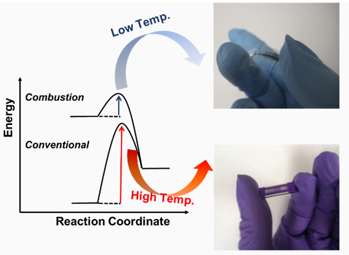
Figure 1. Energetics of combustion synthesis-based processes versus conventional processes. Optical image of a flexible combustion-processed In2O3 device on AryLite (30 nm Al gate electrode/41 nm a-alumina dielectric, with 30 nm Al source and drain electrodes) compared to the one with sol-gel processed on Si substrate.
Polymer incorporation in metal oxides
Polymer incorporation in metal oxide matrices holds the potential to yield enhanced performance on solution processed metal oxide. Incorporating the functionalities of polymers into MO semiconductors can be achieved, leading to metal oxide transistors with mechanical flexibility, transparency, and high mobility. Moreover, polymer incorporation is an effective way to manipulate the solution rheological properties, making the precursors compatible with various printing techniques, including blade-coating, aerosol jet printing, and brush printing.
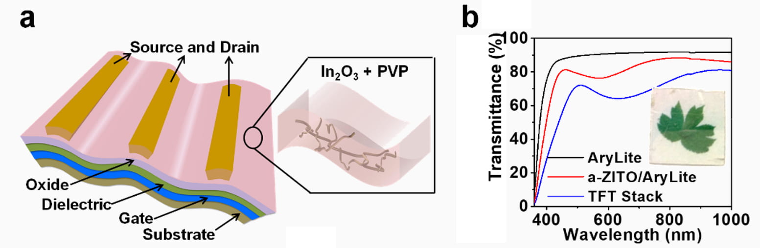
Figure 2. (a) Schematic representation of the flexible, transparent TFT structure and of the metal oxide:polymer (In2O3:x%PVP) semiconductor blend. (b) Optical transmittance spectra of the AryLite substrate, a-ZITO coated AryLite, and the entire TFT stack; the inset shows the optical image of a TFT array on top of a leaf image.
Thin Film Applications in Electronic Devices
Thin Film transistors (TFTs)
Solution-processing metal oxide (MO) films at low temperature enables their integration in mechanically flexible and inexpensive substrates for unconventional optoelectronics. However, temperature reduction has not been accompanied by a corresponding reduction in film-processing time, which remains far greater than acceptable for efficient/continuous additive manufacturing as in typical fabrication lines. Here, we report a highly efficient cofuel-assisted combustion process, which involves introducing both a fluorinated fuel and a pre-annealing step, that achieves ultrafast reaction and metal–oxygen–metal (M-O-M) lattice condensation within 10–60 s for several MO semiconductors and aluminum oxide dielectric. The resulting MO transistors exhibit high carrier mobility, excellent bias stability, and good flexibility.
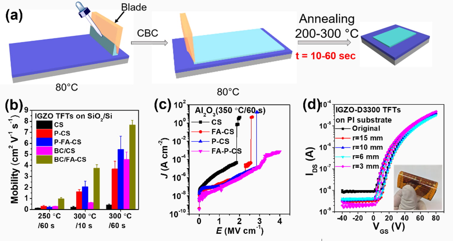
Figure 4. (a) Bladed coating film-fabrication. (b) IGZO TFT mobilities on 300-nm SiO2/Si, and (c) leakage current-density versus electrical field (J-E) of Al2O3 dielectrics fabricated by the indicated methods. (d) Transfer curves of top-gate flexible CBC/IGZO TFTs on a PI substrate as a function of bending radius. Combustion synthesis (CS), fuel-assisted CS (FA-CS), pre-annealed CS (P-CS), and pre-annealed FA-CS (P-FA-CS) processes; BC/CS, blade coating/combustion synthesis; BC/FA-CS, blade coating/fuel-assisted combustion synthesis; CBC, combustion blade coating.
High‐performance solution‐processed metal oxide (MO) thin‐film transistors (TFTs) are realized by fabricating a homojunction of indium oxide (In2O3) and polyethylenimine (PEI)‐doped In2O3 (In2O3:x% PEI, x = 0.5–4.0 wt%) as the channel layer. A two‐dimensional electron gas (2DEG) is thereby achieved by creating a band offset between the In2O3 and PEI‐In2O3 via work function tuning of the In2O3:x% PEI, from 4.00 to 3.62 eV as the PEI content is increased from 0.0 (pristine In2O3) to 4.0 wt%, respectively. The resulting devices achieve electron mobilities greater than 10 cm2V−1s−1 on a 300 nm SiO2 gate dielectric. Importantly, these metrics exceed those of the devices composed of the pristine In2O3 materials, which achieve a maximum mobility of ≈4 cm2V−1s−1. Furthermore, a mobility as high as 30 cm2V−1s−1 is achieved on a high‐k ZrO2 dielectric in the homojunction devices. This is the first demonstration of 2DEG‐based homojunction oxide TFTs via band offset achieved by simple polymer doping of the same MO material.
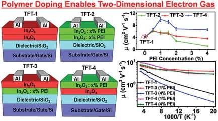
Figure 5. Homojunction oxide thin‐film transistors (TFTs) are realized by combining pristine In2O3 and polyethylenimine (PEI)‐doped In2O3 as a bilayer TFT channel, affording excellent transistor performance. The optimal PEI doping concentration of 1–1.5 wt% affords electron mobilities of >10 and 30 cm2V−1s−1 on a SiO2 or ZrO2 gate dielectric, respectively, which are ≈2× those of pristine In2O3 TFTs.
Perovskite Solar Cells (PSCs)
Perovskite solar cells (PSCs) have advanced rapidly with power conversion efficiencies (PCEs) now exceeding 22%. Due to the long diffusion lengths of charge carriers in the photoactive layer, a PSC device architecture comprising an electron‐ transporting layer (ETL) is essential to optimize charge flow and collection for maximum performance. Here, a novel approach is reported to low temperature, solution‐processed ZnO ETLs for PSCs using combustion synthesis. Due to the intrinsic passivation effects, high crystallinity, matched energy levels, ideal surface topography, and good chemical compatibility with the perovskite layer, this combustion‐derived ZnO enables PCEs approaching 17–20% for three types of perovskite materials systems with no need for ETL doping or surface functionalization.
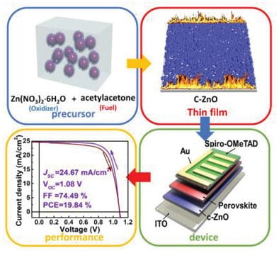
Figure 6. An effective approach to low temperature, solution‐processed ZnO electron‐transport layers (ETLs) for perovskite solar cells by combustion synthesis is developed. Due to the intrinsic passivation effects, high crystallinity, matched energy levels, ideal surface topography, and good chemical compatibility with the perovskite layer, combustion‐processed ZnO electron transport layers enable power conversion efficiencies approaching 17–20% for three representative perovskite systems without ETL doping or surface functionalization.
Collaborations
The C-team also actively contributes to many collaborating projects. We cooperate with material scientists, theorists, physicists, and electrical engineers from Northwestern, Argonne, NIST, Missouri University of Science and Technology and Florida State University, et.al.
Featured Covers