
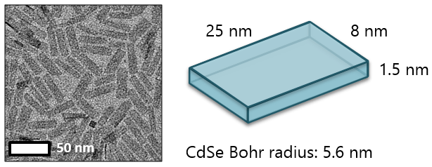
It has recently become possible to synthetically control the growth of colloidal semiconductor materials to produce nanoparticles with atomically precise thicknesses of a few monolayers. These materials, called nanoplatelets (NPLs), experience quantum confinement in only a single dimension; as a result, their ensembles exhibit uniform electronic characteristics. The narrow emission and high absorption cross-section of NPLs — partially a result of their large surface areas — makes them useful for optoelectronic applications such as light-emitting diodes, lasers, solar cells, and photocatalysts that rely on charge and energy transfer processes to function.
 To probe these processes, our group uses time-resolved photoluminescence. Our streak camera can offer resolution up to 1-2 ps, such that charge and energy transfer on a picosecond timescale can be resolved. By comparing the dynamics of particles as independent species (either an isolated donor or acceptor) or in mixtures with a donor or acceptor, the lifetime of charge or energy transfer can be determined. We have used this method to study charge and energy transfer as a function of lateral size and dimensionality, comparing the rates of these electronic processes in two-dimensional NPLs of varying sizes to those in zero-dimensional quantum dots. To probe these processes, our group uses time-resolved photoluminescence. Our streak camera can offer resolution up to 1-2 ps, such that charge and energy transfer on a picosecond timescale can be resolved. By comparing the dynamics of particles as independent species (either an isolated donor or acceptor) or in mixtures with a donor or acceptor, the lifetime of charge or energy transfer can be determined. We have used this method to study charge and energy transfer as a function of lateral size and dimensionality, comparing the rates of these electronic processes in two-dimensional NPLs of varying sizes to those in zero-dimensional quantum dots.
|
 On a more applied level, we have contributed to research showing that NPLs are promising gain media for lasers. We have shown that both CdSe and CdS NPLs exhibit low amplified spontaneous emission thresholds, in particular for lasers emitting at blue wavelengths. On a more applied level, we have contributed to research showing that NPLs are promising gain media for lasers. We have shown that both CdSe and CdS NPLs exhibit low amplified spontaneous emission thresholds, in particular for lasers emitting at blue wavelengths.
|